In the fast-evolving world of electronics, visiting a modern PCB (Printed Circuit Board) factory can be both exciting and insightful. Whether you’re an OEM, engineer, or procurement specialist, understanding what happens behind the scenes of PCB manufacturing can help you make informed decisions, assess production quality, and build better partnerships. Here’s a detailed guide on what to expect when you step into a cutting-edge PCB facility.
1. State-of-the-Art Infrastructure
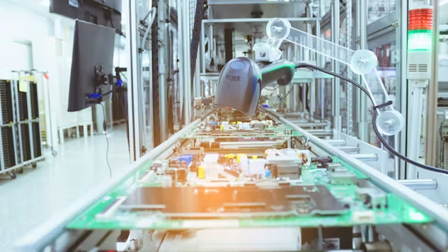
Modern PCB factories are equipped with high-tech machinery, cleanroom environments, and automated production lines. From multilayer PCB fabrication to surface mount technology (SMT) assembly, the PCBA Factory floor is often designed for precision, speed, and scalability.
Expect to see:
-
CNC drilling and laser cutting machines
-
Automated Optical Inspection (AOI) systems
-
SMT pick-and-place lines
-
Reflow and wave soldering equipment
-
Environmental testing and quality control labs
Many facilities also feature ESD-protected areas to prevent electrostatic damage to sensitive components.
2. Focus on Quality Assurance
One of the hallmarks of a reputable PCB manufacturer is a rigorous quality management system. During your visit, you’ll likely observe:
-
Incoming material inspections
-
In-line testing procedures (ICT, flying probe, AOI, X-ray)
-
Functional testing of assembled PCBs
-
ISO certifications such as ISO 9001, ISO 14001, or IATF 16949
You may also be shown real-time production dashboards displaying yield rates, defect analysis, and batch tracking—demonstrating transparency and process control.
3. Eco-Friendly and Safe Manufacturing
Modern PCB factories are increasingly eco-conscious, incorporating wastewater treatment systems, recycling programs, and energy-efficient machinery. You might see:
-
Lead-free soldering processes (RoHS compliant)
-
Chemical waste management units
-
Air filtration systems
-
Solar energy integration
Expect strict adherence to health and safety protocols, including PPE requirements, hazard signage, and emergency preparedness plans.
4. End-to-End Manufacturing Capabilities
Many factories today offer one-stop PCB solutions, from design and prototyping to mass production and assembly. During your tour, you may be introduced to departments such as:
-
PCB Design and Engineering Support
-
Prototyping and NPI (New Product Introduction)
-
SMT & Through-Hole Assembly
-
Box Build and Final Assembly
-
Supply Chain and Logistics
Having these services under one roof improves time-to-market and minimizes communication gaps between stages.
5. Digital Integration and Smart Manufacturing
With the rise of Industry 4.0, expect to witness smart factory elements like:
-
ERP & MES systems integration
-
Real-time production monitoring
-
Predictive maintenance tools
-
Digital twin technology
These innovations not only improve efficiency and consistency but also give you as a customer greater visibility into the production lifecycle.
6. Customer-Centric Experience
A modern PCB manufacturer will prioritize customer satisfaction. Your visit might include:
-
A detailed presentation of company capabilities
-
A guided tour tailored to your interests (e.g., HDI, flexible PCBs, automotive PCBs)
-
Face-to-face time with project managers or engineers
-
Sample reviews and past project showcases
Some factories also provide co-working lounges or meeting rooms, allowing you to discuss projects and ask technical questions on-site.
Final Thoughts: Why a Factory Visit Matters
Visiting a PCB factory is more than just a tour—it’s a strategic step toward building trust and verifying capabilities. You gain firsthand insights into their technical strengths, operational standards, and commitment to quality. For businesses looking to establish long-term partnerships, a visit can reveal whether a manufacturer is equipped to handle both current and future demands.